Tag Archives: efficiency

ADC Energy Efficiency Trends


Fig. 1. State-of-the-art energy per sample vs. ENOB in five-year steps from 1983 to 2013.

Fig. 1. State-of-the-art energy per sample vs. ENOB in five-year steps from 1983 to 2013.

ADC ENERGY EFFICIENCY EVOLUTION: What are the trends for ADC energy efficiency and why did the “Walden” figure-of-merit get almost canonical status when it doesn’t fit to current data? Read on, and you’ll know.

Evolution front

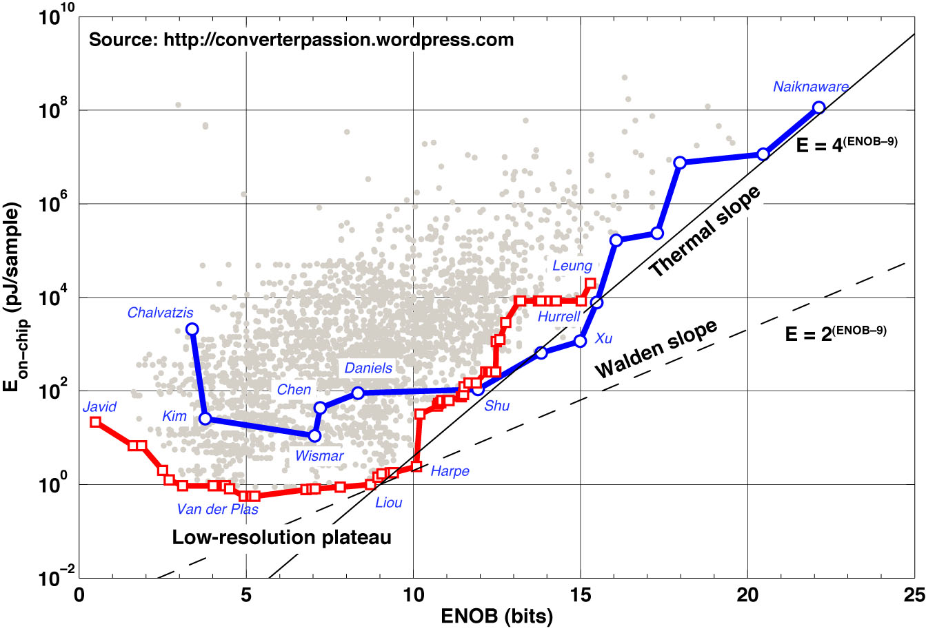
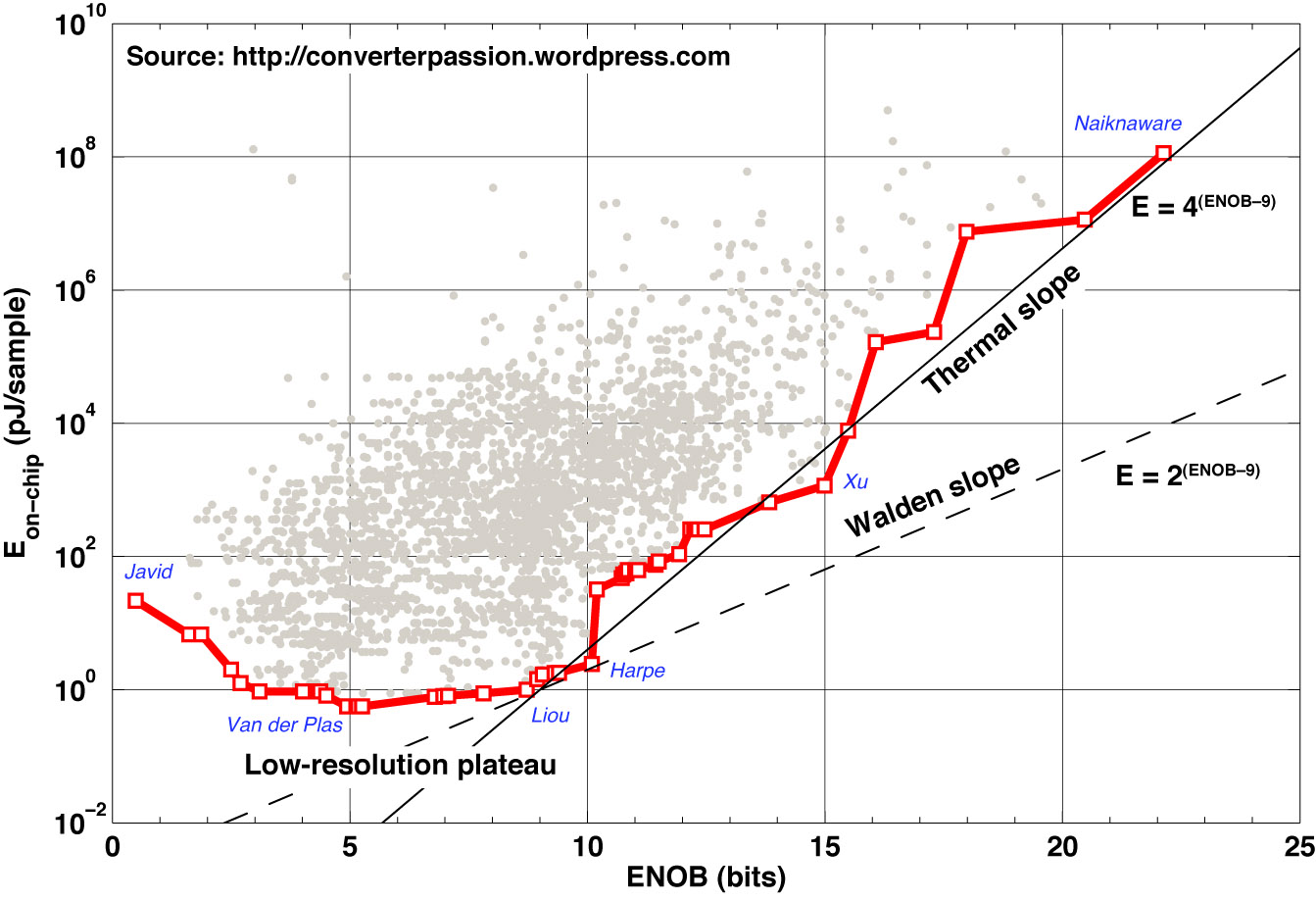
Figure 1 shows how the state-of-the-art boundary for energy-per-sample (Es) vs. effective-number-of-bits (ENOB) has progressed over time in 5-year steps from 1983 to 2013. The energy vs. resolution dependencies suggested by the Walden and Thermal figures-of-merit (FOM) have been indicated as the Walden and Thermal slope, respectively.

Snow cone scatter

The most immediately striking feature in Fig. 1 is that the curves are increasingly more separated at lower resolutions, and tend to group more closely together as ENOB increases. With the Thermal and Walden slopes overlaid as in Fig. 1, you get a kind of “snow cone scatter plot”. It means that the energy efficiency has improved far more for low-resolution ADCs than for high-resolution converters during the 30 years of research covered by Fig. 1. A possible explanation for that is the fairly low number of attempts reported above 15-b ENOB. Another reason could be that the power dissipation at ultra-high resolution almost inevitably becomes limited by thermal noise constraints, and that the few reported designs were carefully optimized. As an example, the work by Naiknaware et al. [1] is the only scientific ADC reporting an ENOB > 20-b (other works only report static linearity or measures that did not resolve to an SNDR value). Although Naiknaware’s design was reported as early as year 2000, it is still on par with today’s noise-limited state-of-the-art. That’s quite impressive!

Slope twist

A second distinct feature in Fig. 1 is that the slope for Es vs. ENOB has changed over time from an almost perfect Walden FOM model (doubling of Es per additional bit) to an almost perfect Thermal FOM model (quadrupling of Es per additional bit).

This explains the great mystery of the Walden FOM and its near-canonical status: Even as late as 2003, the state-of-the-art edge aligned very well with a Walden model. In fact, the Walden model remained true to empirical data all the way to 2007. By 2008, however, the experimental data had started to break away from the Walden slope – something that was also noted by Murmann in his well-known CICC 2008 paper [2] – and by 2013 the experimental data fits more or less perfectly with the thermal-noise model.

The van Elzakker leap

The single most influential contribution to this shift is probably that by van Elzakker et al. [3] as it represented nothing less than a quantum leap in energy efficiency for ADCs in the lower mid-range of resolutions. It gave us a new experimental data-point that completely redefined the energy landscape as it showed their medium-resolution design to be pushed all the way to the thermal-noise power limit of 2008. I believe their contribution broke a mental barrier for many regarding how far you can actually go, and what is the real energy limit. Over the last five years, other authors have followed by reporting more experimental data – both filling the gap created by the van Elzakker leap and pushing efficiency even further [4]-[6].

Low-resolution plateau

As always, we have the low-resolution plateau. There is a slight tendency towards a plateau already in the 1998 curve, and by 2003 it was fully visible – although at a much higher Es level than today’s plateau. Figure 1 also shows us that there has been significant progress at resolutions below 9-b over the 20 years from 1988 to 2008, but almost no movement at all during the last 5 years. The relative amount of attempts below 9-b (~35%) has remained the same both before and after 2008, so it should not be due to lack of interest.

Any explanations you might have would be very interesting to hear. Pure speculations are fine too 😉

Hopes and expectations for the future

In coming years I would expect to see progress in the 10–13 bit region, which seems to be a bit underexplored at the moment. We saw an extension in this direction by the most recent state-of-the-art work by Harpe et al. [4]. I hope that future authors will continue to push the resolution for ultra-efficient ADCs. It should be possible to “iron out the wrinkles” on the current state-of-the-art border. It would be particularly nice if we could populate the border with evenly spaced SAR implementations spanning all the way up to the high resolution of commercial SAR ADCs.

I also hope that someone will explore the empty space below the low-resolution plateau. It seems to be a lot of data points missing there that could give us a better understanding of the true energy limits.

More data at ultrahigh resolution – please!

Finally, I want to plead to those of you designing ultrahigh resolution ADCs to start including traditional dynamic performance measures (at least SNDR) even if the target application you’re imagining doesn’t care about it. If nothing else, it would increase your visibility in my scatter plots, but the main benefit for our science is that we would get more experimental data and a better understanding of the design space for “20-b and beyond”.

So, please … 🙂

References

  1. R. Naiknaware, and T. Fiez, “142dB ∆∑ ADC with a 100nV LSB in a 3V CMOS Process,” Proc. of IEEE Custom Integrated Circ. Conf. (CICC), Orlando, USA, pp. 5-8, May, 2000.
  2. B. Murmann, “A/D converter trends: Power dissipation, scaling and digitally assisted architectures,” Proc. of IEEE Custom Integrated Circ. Conf. (CICC), San Jose, California, USA, pp. 105–112, Sept., 2008.
  3. M. van Elzakker, E. van Tuijl, P. Geraedts, D. Schinkel, E. Klumperink, and B. Nauta, “A 1.9μW 4.4fJ/Conversion-step 10b 1MS/s charge-redistribution ADC,” Proc. of IEEE Solid-State Circ. Conf. (ISSCC), San Francisco, California, pp. 244–245, Feb., 2008.
  4. C.-Y. Liou, and C.-C. Hsieh, “A 2.4-to-5.2fJ/conversion-step 10b 0.5-to-4MS/s SAR ADC with Charge-Average Switching DAC in 90nm CMOS,” Proc. of IEEE Solid-State Circ. Conf. (ISSCC), San Francisco, USA, pp. 280–281, Feb., 2013.
  5. P. Harpe, E. Cantatore, and A. van Roermund, “A 2.2/2.7fJ/conversion-step 10/12b 40kS/s SAR ADC with Data-Driven Noise Reduction,” Proc. of IEEE Solid-State Circ. Conf. (ISSCC), San Francisco, USA, pp. 270–271, Feb., 2013.
  6. H.-Y. Tai, H.-W. Chen, and H.-S. Chen, “A 3.2fJ/c.-s. 0.35V 10b 100KS/s SAR ADC in 90nm CMOS,” Symp. VLSI Circ. Digest of Technical Papers, Honolulu, USA, pp. 92–93, June, 2012.

ADC Energy Efficiency: Nyquist vs. DSM


Fig. 1. Scientific ADC research: On-chip energy per sample vs. ENOB. Current state-of-the-art highlighted for Nyquist ADCs and ∆∑-modulators.

Fig. 1. Scientific ADC research: On-chip energy per sample vs. ENOB. Current state-of-the-art highlighted for Nyquist ADCs and ∆∑-modulators.

ADC ENERGY EFFICIENCY: As a complement to the previous post, the energy vs. resolution is compared for Nyquist ADCs and ∆∑-modulators (DSM) in this post.

Class differences

Although it’s good to get an overall view of the landscape first, the previous post didn’t reveal any detail other than the basic shape, and the state-of-the-art border or envelope. We can get additional insight if we divide the data set by A/D-converter class. Every converter has been sorted into one of five classes:

  • Asynchronous
  • ∆∑-modulator
  • Nyquist
  • Narrow-band
  • Other

Asynchronous means truly asynchronous, and does not include ADCs where the input is synchronously sampled and only the conversion is self-timed or ripple-through. Narrow-band is any converter other than ∆∑ for which the dynamic performance was calculated over a bandwidth lower than fs/2. Other is obviously the catch-all class for anything that didn’t fit in the other four.

Nearly all the data is in the DSM and Nyquist classes, so I have only used those two classes to render the Es vs. ENOB plot in Fig. 1. The global envelope is entirely defined by DSM and Nyquist converters. The envelope corner points [1]-[6] from the previous post are still annotated with first-author names, and a few more that are interesting for this discussion have been added as well [8]-[14].

As you can see from Fig. 1, the two state-of-the-art envelopes have very similar overall form: The energy seems to be limited by thermal noise constraints at higher resolutions, and they both level out to a constant Es, or at least a curve with much less slope at lower resolutions.

The main difference is that the DSM envelope defines the global state-of-the-art at high resolutions, and Nyquist converters define it for low to medium resolution. The transition point is currently at 12-b ENOB. Power-efficient ∆∑-modulators seem to have a noise-limited energy per sample from the 22-b ENOB reported by Naiknaware [6] down to the 12 bits reported by Shu [14]. Below 12 bits, the envelope quickly shifts to a much weaker dependency of resolution – not unlike the plateau observed in the previous post.

In comparison, the best Nyquist ADCs follow the thermal-noise energy model (or a slightly steeper slope) from the 15-b ENOB reported for SAR ADCs by Leung [7] and Hurrell [8] to the SAR ADCs reported by Harpe [4] and Liou [3] with 10 and 9-b ENOB, respectively. Below 9-b, I consider the envelope to be almost constant, as discussed in the previous post.

I guess you all observed the keyword SAR in the above paragraph, didn’t you? The SAR architecture defines more or less the entire shape of the Nyquist envelope, even if there are additional architectures along the plateau.

Energy bounds for low-resolution DSM

I hope there will soon be a theoretical analysis like [15] and [16] for ∆∑ too (please let me know if there is one already). Until then, we have to resort to empirical data. As briefly discussed in the previous post, it’s interesting to understand why the envelope breaks away from the thermal noise limit in the way it does, also for DSM. Are we looking at the same matching/min-size limits as suggested in a comment to the previous post. Lack of data? Lack of the “right” attempts? Limited expectations or other psychological barriers?

Since ∆∑-modulators are often viewed as “high-resolution”, I wanted to investigate the possible scarcity of data below the 12-b breakpoint around Shu [14]. Figure 2 shows how the highest ENOB reported in each paper distributes in the underlying data set. Eyeballing the histogram suggests that maybe as much as 40% of the DSM publications report a peak ENOB < 12-b, so “lack of attempts” can probably not explain why the envelope appears to degrade so quickly.

Fig. 2. Distribution of peak ENOB per scientific paper – divided by Nyquist ADCs and ∆∑-modulators.

Fig. 2. Distribution of peak ENOB per scientific paper.

It is beyond the scope of this post to go really deep into the possible reasons for the “plateau-ish” low-resolution region for DSM, but I may return to investigate the composition of experimental data further to see if it can shed some light. For this post I mainly intended to show what the empirical data looks like. I also want to highlight two additional features of the DSM plateau:

  • Es is 1–2 orders of magnitude higher than for Nyquist converters.
  • The low-resolution envelope is defined by more unusual circuit implementations: Modulators presented by Daniels [13], Wismar [11] and Kim [10] are all VCO-based, whereas Chen [12] used a passive ∆∑-loop where only the comparator is active.

Why the 10–100X difference to Nyquist converters, then? From what I can see, most of the Nyquist converters that populate the low-energy envelope are the result of going to great lengths to weed out anything that has static current, and anything that switches faster or more often than it has to. Since the very foundation of oversampling is to evaluate the circuit state much more often than the Nyquist sampling rate, I assume it will be difficult to close the gap between these two envelopes.

But that’s me. Perhaps you have some idea how it could be done, or how to prove it isn’t possible?

As always, you are welcome to share your own thoughts and interpretations of the data.

Further reading

If you are curious to see what a more detailed breakdown by architecture would look like, you may find the plot in [17] interesting. Beware, though, that the data used in [17] does not include the most recent 400 or so papers from the last three years. Also, the plot is no masterpiece of readability 😉

Perhaps I need to do a new architectural study soon.

References

  1. B. Javid, and P. Heydari, “A 4-bit 12GS/s Data Acquisition System-on-Chip Including a Flash ADC and 4-Channel DeMUX in 130nm CMOS,” Proc. of IEEE Custom Integrated Circ. Conf. (CICC), San Jose, California, USA, pp. 1–4, Sept., 2012.
  2. G. Van der Plas and B. Verbruggen, “A 150 MS/s 133 µW 7 bit ADC in 90 nm Digital CMOS,” IEEE J. Solid-State Circuits, Vol. 43, pp. 2631-2640, Dec., 2008.
  3. C.-Y. Liou, and C.-C. Hsieh, “A 2.4-to-5.2fJ/conversion-step 10b 0.5-to-4MS/s SAR ADC with Charge-Average Switching DAC in 90nm CMOS,” Proc. of IEEE Solid-State Circ. Conf. (ISSCC), San Francisco, USA, pp. 280–281, Feb., 2013.
  4. P. Harpe, E. Cantatore, and A. van Roermund, “A 2.2/2.7fJ/conversion-step 10/12b 40kS/s SAR ADC with Data-Driven Noise Reduction,” Proc. of IEEE Solid-State Circ. Conf. (ISSCC), San Francisco, USA, pp. 270–271, Feb., 2013.
  5. J. Xu, X. Wu, M. Zhao, R. Fan, H. Wang, X. Ma, and B. Liu, “Ultra Low-FOM High-Precision ΔΣ Modulators with Fully-Clocked SO and Zero Static Power Quantizers,” Proc. of IEEE Custom Integrated Circ. Conf. (CICC), San Jose, California, USA, pp. 1–4, Sept., 2011.
  6. R. Naiknaware, and T. Fiez, “142dB ∆∑ ADC with a 100nV LSB in a 3V CMOS Process,” Proc. of IEEE Custom Integrated Circ. Conf. (CICC), Orlando, USA, pp. 5-8, May, 2000.
  7. K. Y. Leung, K. Leung, and D. R. Holberg, “A Dual Low Power ½ LSB INL 16b/1Msample/s SAR A/D Converter with on-chip Microcontroller,” Proc. of IEEE Asian Solid-State Circ. Conf. (ASSCC), Hangzhou, China, pp. 51-54, Nov., 2006.
  8. C. P. Hurrell, C. Lyden, D. Laing, D. Hummerston, and M. Vickery, “An 18 b 12.5 MS/s ADC With 93 dB SNR,” IEEE J. Solid-State Circuits, Vol. 45, pp. 2647-2654, Dec., 2010.
  9. T. Chalvatzis, and S. P. Voinigescu, “A 4.5 GHz to 5.8 GHz Tunable ∆∑ Digital Receiver with Q enhancement,” IEEE MTT-S International Microwave Symp. Digest, Atlanta, USA, pp. 193-196, June, 2008.
  10. J. Kim, T.-K. Jang, Y.-G. Yoon, and S. Cho, “Analysis and Design of Voltage-Controlled Oscillator-Based Analog-to-Digital Converter,” IEEE Trans. Circuit and Systems, Pt. I, Vol. 57, pp. 18-30, Jan., 2010.
  11. U. Wismar, D. Wisland, and P. Andreani, “A 0.2V 0.44µW 20 kHz Analog to Digital ∑∆ Modulator with 57 fJ/conversion FoM,” Proc. of Eur. Solid-State Circ. Conf. (ESSCIRC), Montreux, Switzerland, pp. 187-190, Sept., 2006.
  12. F. Chen, S. Ramaswamy, and B. Bakkaloglu, “A 1.5V 1mA 80dB Passive ΣΔ ADC in 0.13μm Digital CMOS Process,” Proc. of IEEE Solid-State Circ. Conf. (ISSCC), San Francisco, California, pp. 54-65, Feb., 2003.
  13. J. Daniels, W. Dehaene, M. Steyaert, and A. Wiesbauer, “A 0.02mm2 65nm CMOS 30MHz BW All-Digital Differential VCO-based ADC with 64dB SNDR,” Symp. VLSI Circ. Digest of Technical Papers, Honolulu, USA, pp. 155-156, June, 2010.
  14. Y.-S. Shu, J.-Y. Tsai, P. Chen, T.-Y. Lo, and P.-C. Chiu, “A 28fJ/conv-step CT ΔΣ Modulator with 78dB DR and 18MHz BW in 28nm CMOS Using a Highly Digital Multibit Quantizer,” Proc. of IEEE Solid-State Circ. Conf. (ISSCC), San Francisco, USA, pp. 268–269, Feb., 2013.
  15. T. Sundström, B. Murmann, and C. Svensson, “Power dissipation bounds for high-speed Nyquist analog-to-digital converters,” IEEE Trans. Circuits and Systems, pt. I, vol. 56, no. 3, pp. 509–518, Mar. 2009.
  16. D. Zhang, C. Svensson, and A. Alvandpour, “Power consumption for SAR ADCs,” Proc. of Eur. Conf. Circ. Theory and Design (ECCTD), Linköping, Sweden, pp. 556–559, Aug., 2011.
  17. B. E. Jonsson, “An empirical approach to finding energy efficient ADC architectures,” Proc. of 2011 IMEKO IWADC & IEEE ADC Forum, Orvieto, Italy, June 2011. [PDF @ IMEKO]

ADC Energy Efficiency: An empirical overview


Scientific ADC research: On-chip energy per sample vs. ENOB. Current state-of-the-art highlighted.

Scientific ADC research: On-chip energy per sample vs. ENOB. Current state-of-the-art highlighted.

ADC ENERGY EFFICIENCY LIMITS (Updated): A significant part of the ADC community seems to be focused on improving the energy efficiency of data converters. Essentially getting the same job done at ever decreasing energy costs. I’m sure that many of you are trying to figure out what is the absolute limit in the power-performance trade-off. Is it only our imagination or will thermal noise or some other law of physics finally stop us from improving the energy efficiency of ADCs? Well, I will not claim to give the full answer to that. What we will do, however, is to take an empirical look at where the field is today, check if the current state-of-the-art boundaries resemble any familiar theory, and observe how the energy efficiency is influenced by certain design choices and parameters. Since that might be a rather hefty undertaking, we will start out slow and let it all evolve over several blog posts.

What is “energy efficiency”?

First of all, we need to define how to measure energy efficiency. Energy efficiency in this context is about the trade-off between the performance you get and the power you burn. Performance typically means the simultaneous combination of speed and resolution. We will use the equivalent Nyquist sampling rate (fs) to measure speed, and the effective-number-of-bits (ENOB) to measure resolution.

(1) : ENOB = \dfrac{SNDR - 1.76}{6.02}

In order to evaluate the success of power-performance trade-offs, a large number of figures-of-merits (FOM) have been proposed in the literature [1]. A common feature of many FOM is that the power dissipation is normalized by the sampling rate into the expression energy-per-sample

(2) : E_s= \dfrac{P}{f_s}

The starting point for this treatment will therefore be to look at Es vs. ENOB, as plotted in Fig. 1.

The ADC energy landscape

Figure 1 gives a helicopter view of the ADC energy landscape. It shows the energy-per-sample vs. effective resolution for nearly all implementations reported scientifically since 1974 and to this date. The current state-of-the-art envelope is highlighted, and key corner points are indicated with first-author names [2]-[7].

The energy slopes

Two lines have been superimposed as visual guides, and to support the discussion: As mentioned in various publications, e.g., [8]-[11], the power dissipation will quadruple for every effective bit of resolution if the ADC power is limited by thermal noise constraints (e.g., kT/C capacitor sizing), and the architecture is otherwise unchanged [12]. The solid line is therefore

(3) : E_{s} = {4}^{ENOB - 9}\:\textup {pJ}

and has been labeled the Thermal slope. It is equivalent to a constant Thermal FOM

(4) : F_{B1} = \dfrac{P}{{2}^{2\times ENOB}\times f_{s}}\approx{3.8}\:\textup {aJ}

The second visual guide (dashed) is

(5) : E_{s} = {2}^{ENOB - 9}\:\textup {pJ}

and was labeled the Walden slope because it corresponds to a doubling of power dissipation for every additional bit of resolution, as suggested by the Walden FOM. The dashed line corresponds to a constant Walden FOM

(6) : F_{A1} = \dfrac{P}{{2}^{ENOB}\times f_{s}}\approx{2.0}\:\textup {fJ}

The term “–9” is arbitrarily chosen in order to get expressions that are easy to remember and that intersect Es = 1 pJ @ ENOB = 9-b, which is a relevant energy point approximately on the state-of-the-art border.

The low-resolution plateau

As seen in Fig. 1, energy-per-sample levels out to an almost constant value for low resolutions. This Low-resolution plateau is rather puzzling. While degradation below 3-b may be due to lack of data, it doesn’t appear to be any lack of attempts between 3–8 bits. Intuitively, I would not expect Es to be practically independent of ENOB from 8-b and below. Would you? I would expect it to continue to decrease with resolution, but possibly at a slower rate than the thermal slope dictates.

I do have some thoughts on how this may depend on what ADC specs scientists have chosen to target, but it would be very interesting to hear your thoughts on the plateau.

The empirical data vs. the slopes

The “slopes” in Fig. 1 represent the energy-vs.-performance models suggested by the two figures-of-merit FA1 and FB1. As you can see, the thermal slope aligns very well with the state-of-the-art boundary for ENOB ≥ 9-b. There is a fair amount of randomness in the state-of-the-art progress that causes it to zigzag around the ideal model, but the thermal-noise energy model seems to be able to predict the overall slope of the curve from 9-b and above. This should be quite uncontroversial, as it is commonly understood that the power dissipation of high-resolution ADCs is limited by thermal-noise constraints. It should however be noted that recent works seem to extend this relation even to resolutions as low as 9–10-b ENOB.

Regarding the Walden slope, my interpretation is that it fails to fit to the empirical data within in any significant range of resolution, except possibly for the roughly 1-b wide region between Liou [4] and Harpe [5] where the overall curve (according to my interpretation) is in a state of transition from thermal-noise limited to approximately constant. There is also a region between 10–15 bits where the slope is almost identical to the Walden model. To the best of my understanding, this is an inevitable effect of zigzagging around the thermal slope: Locally, the curve will alternate between segments with a more shallow slope (looking like Walden) and segments with a slope even steeper than predicted by the thermal-noise model.

Since I can’t unambiguously prove the above at this point, and since I know this can be a bit sensitive, I will remain open to the possibility that the Walden energy model could still be valid over some range of resolutions.

Please fee free to share your own thoughts and interpretations of the data.

Update: I clearly forgot to mention the theoretical predictions of SAR ADC energy bounds by Zhang, Svensson, and Alvandpour in [13]. Kind of a SAR version of [10]. Since SAR ADCs dominate large segments of the low-energy scene, the paper is extremely relevant to this post. On top of it, the theoretical predictions align very well with the empirical data in Fig. 1 above. (You can try yourself to overlay the two plots in Photoshop or similar)

Upcoming posts

In a few more posts on this topic, I intend to illustrate how the empirically observed ADC efficiency limits depend on parameters such as sampling rate, process node and year.

References

  1. B. E. Jonsson, “Using Figures-of-Merit to Evaluate Measured A/D-Converter Performance,” Proc. of 2011 IMEKO IWADC & IEEE ADC Forum, Orvieto, Italy, June 2011. [PDF @ IMEKO]
  2. B. Javid, and P. Heydari, “A 4-bit 12GS/s Data Acquisition System-on-Chip Including a Flash ADC and 4-Channel DeMUX in 130nm CMOS,” Proc. of IEEE Custom Integrated Circ. Conf. (CICC), San Jose, California, USA, pp. 1–4, Sept., 2012.
  3. G. Van der Plas and B. Verbruggen, “A 150 MS/s 133 µW 7 bit ADC in 90 nm Digital CMOS,” IEEE J. Solid-State Circuits, Vol. 43, pp. 2631-2640, Dec., 2008.
  4. C.-Y. Liou, and C.-C. Hsieh, “A 2.4-to-5.2fJ/conversion-step 10b 0.5-to-4MS/s SAR ADC with Charge-Average Switching DAC in 90nm CMOS,” Proc. of IEEE Solid-State Circ. Conf. (ISSCC), San Francisco, USA, pp. 280–281, Feb., 2013.
  5. P. Harpe, E. Cantatore, and A. van Roermund, “A 2.2/2.7fJ/conversion-step 10/12b 40kS/s SAR ADC with Data-Driven Noise Reduction,” Proc. of IEEE Solid-State Circ. Conf. (ISSCC), San Francisco, USA, pp. 270–271, Feb., 2013.
  6. J. Xu, X. Wu, M. Zhao, R. Fan, H. Wang, X. Ma, and B. Liu, “Ultra Low-FOM High-Precision ΔΣ Modulators with Fully-Clocked SO and Zero Static Power Quantizers,” Proc. of IEEE Custom Integrated Circ. Conf. (CICC), San Jose, California, USA, pp. 1–4, Sept., 2011.
  7. R. Naiknaware, and T. Fiez, “142dB ∆∑ ADC with a 100nV LSB in a 3V CMOS Process,” Proc. of IEEE Custom Integrated Circ. Conf. (CICC), Orlando, USA, pp. 5-8, May, 2000.
  8. A. M. A. Ali, C. Dillon, R. Sneed, A. S. Morgan, S. Bardsley, J. Kornblum, and L. Wu, “A 14-bit 125 MS/s IF/RF sampling pipelined ADC with 100 dB SFDR and 50 fs jitter,” IEEE J. Solid-State Circuits, Vol. 41, pp. 1846–1855, Aug, 2006.
  9. B. Murmann, “A/D converter trends: Power dissipation, scaling and digitally assisted architectures,” Proc. of IEEE Custom Integrated Circ. Conf. (CICC), San Jose, California, USA, pp. 105–112, Sept., 2008.
  10. T. Sundström, B. Murmann, and C. Svensson, “Power dissipation bounds for high-speed Nyquist analog-to-digital converters,” IEEE Trans. Circuits and Systems, pt. I, vol. 56, no. 3, pp. 509–518, Mar. 2009.
  11. B. E. Jonsson, “An empirical approach to finding energy efficient ADC architectures,” Proc. of 2011 IMEKO IWADC & IEEE ADC Forum, Orvieto, Italy, June 2011. [PDF @ IMEKO]
  12. K. Bult, “Embedded analog-to-digital converters,” Proc. of Eur. Solid-State Circ. Conf. (ESSCIRC), Athens, Greece, pp. 52–60, Sept., 2009.
  13. D. Zhang, C. Svensson, and A. Alvandpour, “Power consumption for SAR ADCs,” Proc. of Eur. Conf. Circ. Theory and Design (ECCTD), Linköping, Sweden, pp. 556–559, Aug., 2011.

ADC performance evolution: Walden figure-of-merit (FOM)


Figure 1. Evolution of best reported Walden FOM for delta-sigma modulators (o) and Nyquist ADCs (#). Monotonic state-of-the-art improvement trajectories have been highlighted. Trend fit to DSM (dotted), and Nyquist (dashed) state-of-the-art. Average trend for all designs (dash-dotted) included for comparison.

POWER EFFICIENCY TRENDS: A series of blog posts on A/D-converter performance trends would not be complete without an analysis of figure-of-merit (FOM) trends, would it? We will therefore take a look at the two most commonly used FOM, starting with the by far most popular:

(1) : F_{A1} = \dfrac{P}{{2}^{ENOB}\times f_{s}}

where P is the power dissipation, fs is Nyquist sampling rate, and ENOB is the effective number of bits defined by the signal-to-noise and-distortion ratio (SNDR) as:

(2) : ENOB = \dfrac{SNDR - 1.76}{6.02}

FA1 is sometimes referred to as the Walden or ISSCC FOM and relates the ADC power dissipation to its performance, represented by sampling rate and conversion error amplitude. The best reported FA1 value each year has been plotted for delta-sigma modulators (DSM) and Nyquist ADCs in Fig. 1. Trajectories for state-of-the-art have been indicated, and trends have been fitted to these state-of-the-art data points. The average improvement trend for all ADCs (2×/2.6 years) is included for comparison.

By dividing the data into DSM and Nyquist subsets, it is seen that delta-sigma modulators have improved their state-of-the-art FOM at an almost constant rate of 2×/2.5 years throughout the existence of the field – just slightly faster than the overall average. State-of-the-art Nyquist ADCs have followed a steeper and more S-shaped evolution path. Their overall trend fits to a 2× improvement every 1.8 years, although it is obvious that evolution rates have changed significantly over time. A more accurate analysis of Nyquist ADC trends should probably make individual fits of the early days glory, the intermediate slowdown, and the recent acceleration phase. This was done in [1] where evolution was analyzed with DSM and Nyquist data merged. However, for simplicity I’ll just stick to the more conservative overall Nyquist trend. [I wouldn’t want anyone to suggest that I’m producing “subjective” or “highly speculative” trend estimates, would I? 😉 ]

Still, if anyone is curious to know … 🙂 … the state-of-the-art data points fit to a 2×/14 months trend between 2000 and 2010. That’s actually faster than Moore’s Law, which is traditionally attributed a 2×/18 months rate [2]-[3]. A new twist on “More than Moore”, perhaps? Even the more conservative overall 2×/21 months trend is close enough to conclude that the state-of-the-art FOM for Nyquist ADCs has developed exponentially in a fashion closely resembling Moore’s Law. And that’s got to be an impressive trend for any analog/mixed circuit performance parameter.

Irrespective of what’s the best fit to data, it should be evident from Fig. 1 that Nyquist ADCs broke away from the overall trend around year 2000, and has since followed a steeper descent in their figures-of-merit. They have also reached further (4.4 fJ) [4] than DSM (35.6 fJ) [5]. The overall trend projects to a 0.2 fJ ADC FOM in 2020. Whether or not that’s possible, we’ll leave for another post. A deeper look at the data also reveals that:

  • The acceleration in state-of-the-art is almost completely defined by successive-approximation (SAR) ADCs [4], [6]-[11], accompanied by a single cyclic ADC [12]. The superior energy efficiency of the SAR architecture was empirically shown in [13].
  • A significant part of the acceleration can be explained by the increased tendency to leave out, for example I/O power dissipation when reporting experimental results – a trend also observed by Bult [14]. The FOM in the graph was intentionally calculated from the on-chip rather than total power dissipation because: (a) ADCs are increasingly used as a system-on-chip (SoC) building block, which makes the stand-alone I/O power for a prototype irrelevant, and (b) Many authors don’t even report the I/O power anymore.
  • FA1 has a bias towards low-power, medium resolution designs rather than high-resolution, and thus benefits from CMOS technology scaling as shown in [15],[16]. An analysis of the underlying data shows that, for the best FA1 every year, the trajectories for ENOB and P follows distinct paths towards consistently lower power and medium resolution. You simply gain more in FA1 by lowering power dissipation than by increasing resolution because (1) does not correctly describe the empirically observed power-resolution tradeoff for ADCs [13],[15].

In order to compare high-resolution ADCs limited by thermal noise, it has therefore been proposed to use a slightly different FOM, sometimes labeled the “Thermal FOM” [17]-[18],

(3) : F_{B1} = \dfrac{P}{{2}^{2\times ENOB}\times f_{s}}

This figure-of-merit will be the topic of the next post.

See also …

ADC survey data

Walden’s survey [19]

References

  1. B. E. Jonsson, “A survey of A/D-converter performance evolution,” Proc. of IEEE Int. Conf. Electronics Circ. Syst. (ICECS), Athens, Greece, pp. 768–771, Dec., 2010.
  2. G.E. Moore, “Cramming more components onto integrated circuits,” Electronics, Vol. 38, No. 8, Apr. 1965.
  3. G. E. Moore, “No exponential is forever: but “forever” can be delayed!,” IEEE ISSCC, Dig. Tech. Papers, San Francisco, CA, Feb. 2003, pp. 20–23.
  4. M. van Elzakker, E. van Tuijl, P. Geraedts, D. Schinkel, E. Klumperink, and B. Nauta, “A 1.9μW 4.4fJ/Conversion-step 10b 1MS/s Charge-Redistribution ADC,” Proc. of IEEE Solid-State Circ. Conf. (ISSCC), San Francisco, California, pp. 244–245, Feb., 2008.
  5. J. Xu, X. Wu, M. Zhao, R. Fan, H. Wang, X. Ma, and B. Liu, “Ultra Low-FOM High-Precision ΔΣ Modulators with Fully-Clocked SO and Zero Static Power Quantizers,” Proc. of IEEE Custom Integrated Circ. Conf. (CICC), San Jose, California, USA, pp. 1–4, Sept., 2011.
  6. A. Shikata, R. Sekimoto, T. Kuroda, and H. Ishikuro, “A 0.5 V 1.1 MS/sec 6.3 fJ/Conversion-Step SAR-ADC With Tri-Level Comparator in 40 nm CMOS,” IEEE J. Solid-State Circuits, Vol. 47, pp. 1022–1030, Apr., 2012.
  7. T.-C. Lu, L.-D. Van, C.-S. Lin, C.-M. Huang, “A 0.5V 1KS/s 2.5nW 8.52-ENOB 6.8fJ/Conversion-Step SAR ADC for Biomedical Applications,” Proc. of IEEE Custom Integrated Circ. Conf. (CICC), San Jose, California, USA, pp. 1–4, Sept., 2011.
  8. S.-K. Lee, S.-J. Park, Y. Suh, H.-J. Park, and J.-Y. Sim, “A 1.3µW 0.6V 8.7-ENOB Successive Approximation ADC in a 0.18µm CMOS,” Symp. VLSI Circ. Digest of Technical Papers, Honolulu, USA, pp. 242–243, June, 2009.
  9. H.-C. Hong, and G.-M. Lee, “A 65-fJ/Conversion-Step 0.9-V 200-kS/s Rail-to-Rail 8-bit Successive Approximation ADC,” IEEE J. Solid-State Circuits, Vol. 42, pp. 2161–2168, Oct., 2007.
  10. M. D. Scott, B. E. Boser, and K. S. J. Pister, “An Ultra-Low Power ADC for Distributed Sensor Networks,” Proc. of Eur. Solid-State Circ. Conf. (ESSCIRC), Firenze, Italy, pp. 255–258, Sept., 2002.
  11. M. D. Scott, B. E. Boser, and K. S. J. Pister, “An Ultralow-Energy ADC for Smart Dust,” IEEE J. Solid-State Circuits, Vol. 38, pp. 1123–1129, July, 2003.
  12. D. Muthers, and R. Tiekert, “A 0.11mm2 low-power A/D-converter cell for 10b 10MS/s operation,” Proc. of Eur. Solid-State Circ. Conf. (ESSCIRC), Leuven, Belgium, pp. 251–254, Sept., 2004.
  13. B. E. Jonsson, “An empirical approach to finding energy efficient ADC architectures,” Proc. of 2011 IMEKO IWADC & IEEE ADC Forum, Orvieto, Italy, pp. 1–6, June 2011. [PDF @ IMEKO]
  14. K. Bult, “Embedded analog-to-digital converters,” Proc. of Eur. Solid-State Circ. Conf. (ESSCIRC), Athens, Greece, pp. 52–60, Sept., 2009.
  15. B. E. Jonsson, “Using Figures-of-Merit to Evaluate Measured A/D-Converter Performance,” Proc. of 2011 IMEKO IWADC & IEEE ADC Forum, Orvieto, Italy, pp. 1–6, June 2011. [PDF @ IMEKO]
  16. B. E. Jonsson, “On CMOS scaling and A/D-converter performance,” Proc. of NORCHIP, Tampere, Finland, Nov. 2010.
  17. A. M. A. Ali, C. Dillon, R. Sneed, A. S. Morgan, S. Bardsley, J. Kornblum, and L. Wu, “A 14-bit 125 MS/s IF/RF sampling pipelined ADC with 100 dB SFDR and 50 fs jitter,” IEEE J. Solid-State Circuits, Vol. 41, pp. 1846–1855, Aug, 2006.
  18. C. Wulff, and T. Ytterdal, “Design of a 7-bit, 200MS/s, 2mW pipelined ADC with switched open-loop amplifiers in a 65nm CMOS technology,” Proc. of NORCHIP, Aalborg, Denmark, Nov., 2007.
  19. R. Walden, “Analog-to-digital conversion in the early twenty-first century,” Wiley Encyclopedia of Computer Science and Engineering, pp. 126–138, Wiley, 2008.