Tag Archives: CMOS

ADC performance evolution: Low-voltage operation – part 2


VDD evolution over time (scatterplot)

Fig. 1. Supply voltages used for scientifically reported CMOS ADCs over time. Data points representing the evolution of low-voltage state-of-the-art have been highlighted. Trend line fit to 1985-2007 data.

LOW-VOLTAGE EVOLUTION TRENDS: In part 1 of the low-voltage ADC series of posts, we observed the trends for supply voltage (VDD) vs. process scaling (L). In this second post we will complete the picture by looking at VDD trends over time. The timing for introduction of new process technology, and the nominal supply voltage for future nodes, are reasonably well-defined through the continuously updated International Technology Roadmap for Semiconductors (ITRS) [1], but at least two ADC-related aspects are not controlled by the ITRS scaling roadmap:

  • The rate at which mainstream ADC research activities will migrate to newer CMOS technology.
  • To what extent the ADC research community will attempt to push the envelope with respect to ultra-low voltage operation.

Regarding the former, it was observed in a previous post that the number of early adopters for each node is very small. In any year, the absolute majority of experimental ADCs have so far been implemented in technology being 2–5 generations behind the scaling front. How the “mainstream” will behave in the future is next to impossible to predict, as it is influenced by future industrial needs, research grant policies, research community group dynamics, journal and conference publication targets, as well as many other hard and soft parameters of which we know very little today.

The latter depends on a handful of pioneers choosing to explore the outer limits of ultra-low voltage ADC operation. It was seen in part 1 that there have been rather few attempts to push in this direction, which reveals that only a few groups have historically chosen this focus. If no one decides to have a shot at the current world record – the 0.2 V, VCO-based ∑-∆ modulator presented by Wismar et al. in [2] – we may never see it nudged.

It is therefore very difficult to predict the future VDD trends for analog-to-digital converters, both with respect to the ultra-low voltage state-of-the-art, and the mainstream supply voltage. What we can do, however, is to observe historical trends and use them as a reference.

Observation of ADC supply voltage trends

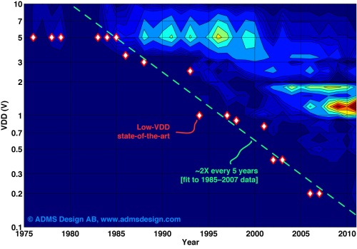
Figure 1 shows the voltage supplies reported for CMOS A/D-converters reported in scientific publications until Q1-2012. The graph shows the highest supply voltage applied to the circuit. It means that, if a circuit used several independent supplies, then VDD = max(VDD1, VDD2, …, VDDn), so that true low-voltage operation is promoted. The evolution of low-voltage state-of-the-art has been highlighted.

A similar graph in [3] shows data for all ADCs (CMOS, as well as bipolar and BiCMOS) but with data only to Q1-2010. Focusing on CMOS, and adding two more years of empirical data yields a different scatter. Nevertheless, the low-voltage state-of-the-art sequence here is nearly identical to that in [3] because the global state-of-the-art  almost completely coincides with CMOS ADCs, and also did not improve since 2006. As observed in [3], the lowest reported VDD remained unchanged at 5 V until 1985, after which it started to follow a noisy but distinct scaling trend for 20 years. Fitting to the state-of-the-art data from 1985–2007, yields that the lowest reported VDD was scaled by ~2× every five years during this period.

Figure 2 shows the distribution of scientific ADC implementations over supply voltage and publication year as a contour plot. The state-of-the-art data points and trend fit from Fig. 1 have been superimposed for reference. Just as in part 1, manually selected bin centers and non-linear contour levels have been used in order to render a meaningful and readable (but simplified) plot. The main purpose is to illustrate the difference between mainstream VDD and state-of-the-art low-voltage operation each year. It is observed that:

  • Mainstream focus remained at 5 V for over 20 years.
  • The state-of-the-art VDD scaling front started to go below 5 V around 12–15 years before any noticeable change in the mainstream focus.
  • The low-voltage scaling front appears to be approximately 5–6× below, and 10–15 years ahead of the mainstream VDD for each year.
  • Supply voltages from 5 V and down seem to have an extremely long lifetime in publications.

What do you observe?
Distribution of VDD over time (contour plot)

Figure 2. Voltage supplies used for scientific ADCs over time. Color represents number of publications. The low-voltage state-of-the-art data points are superimposed along with a scaling trend estimated from 1985–2007 data.

Future VDD scaling for ADCs

I’m very aware that there are good reasons why ultra-low VDD scaling may not be able go much further, so please note that I’m not saying here that it will. Perhaps it is physically impossible, or functionally meaningless to go significantly further than the 200 mV operation achieved by Wismar, et al. On the other hand, I’m old enough to have heard one “hard” limit after another being suggested for MOST scaling, and we’re still scaling them. So, let’s just see where we would end up if it should turn out to be possible also for the voltage supply:

If the current trend for ultra-low voltage ADCs should be maintained, the low-voltage pioneers would have to publish ADCs according to the following approximate schedule:

Year VDD
2015 73 mV
2020 36 mV
2025 18 mV

Again, I’m not saying that it will happen. But I still found it interesting to see what kind of supplies the historical trend is projecting towards. Does anyone dare to predict a hard limit for A/D-converter supply voltage? Do you believe we will ever see an ADC operating at 73 mV? Is 36 mV impossible? What are the possibilities in context of the impossibilities?

In case anyone wish to make their own projections, the trend fit expression is:

VDD = {10}^{-0.061011\times year + 121.7998}

See also …

ADC performance evolution: Low-voltage operation – part 1

ADC research trends: CMOS node adoption

ADC research trends: Migration to CMOS

ADC Survey Data

References

[1] International Technology Roadmap for Semiconductors (ITRS), 2011 Edition [Online]. Available: http://www.itrs.net

[2] U. Wismar, D. Wisland, and P. Andreani, “A 0.2V 0.44µW 20 kHz analog to digital ∑∆ modulator with 57 fJ/conversion FoM”, Proc. of Eur. Solid-State Circ. Conf. (ESSCIRC), Montreux, Switzerland, pp. 187-190, Sept., 2006.

[3] B. E. Jonsson, “A survey of A/D-converter performance evolution,” Proc. of IEEE Int. Conf. Electronics Circ. Syst. (ICECS), Athens, Greece, pp. 768–771, Dec., 2010.

ADC performance evolution: Low-voltage operation – part 1


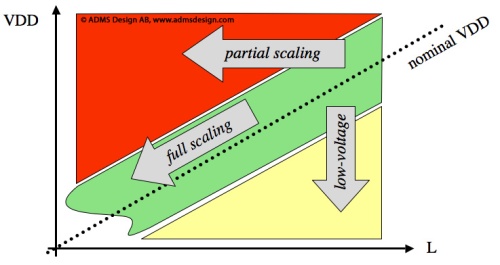
Figure 1. Two-dimensional view of CMOS scaling: Channel length and VDD.

EMBRACING LOW VOLTAGE OPERATION: As analog-to-digital converter implementations migrate to scaled-down CMOS technologies, they also face the inevitable downscaling of supply voltages (VDD), and hence signal swing [1]. A signal chain with a weak signal is more likely to suffer from noise than one with a strong signal. The scaling trends for VDD are therefore important as a background to the A/D-converter noise performance trends that will be treated in a few upcoming posts. There are also other reasons for a circuit designer to keep an eye on the evolution of supply voltage, such as the considerable challenges for high-gain OP-amp design or sampling linearity under low-voltage operation, so I hope you’ll find this post useful even on its own.

Voltage scaling: The stragglers, the mainstream, and the pioneers

Contrary to the minimum channel length (L), we can choose to go lower than the nominal supply voltage specified for a process. Possibly at our own risk, but at least it can be done. It has therefore been possible to scale VDD “ahead” of the node you actually use. Unless you have direct access to a semiconductor fab, you can’t do that with respect to L. This degree of freedom – at least for experimental ADC designs – has lead to the situation illustrated by Fig. 1:

  • Some (or as we shall see below, most) designs use the nominal supply voltage recommended for any given CMOS node.
  • Others may use the same node, but the design is not “fully scaled”. It relies on higher-than-nominal VDD, and possibly optional process steps that effectively recreate older and less scaled device technology as well.
  • A third category not only embraces the full scaling, but actually use a more aggressive scaling of supply voltages. These are the low-voltage pioneers.

This post will observe how supply voltage distribute over CMOS node for scientifically reported ADCs, and attempt to extract evolution trends and trajectories for VDD vs. L.

ADC supply voltage vs. CMOS node

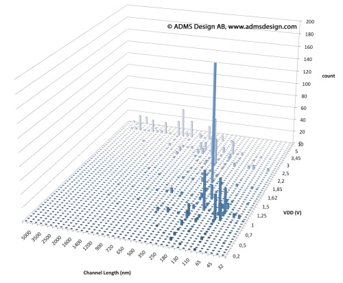
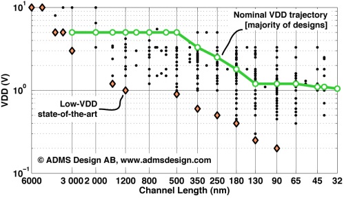
As pointed out in [2], the reported supply voltage can vary as much as one order of magnitude within the same node for scientific A/D-converters. This is illustrated by the scatter plot of {L, VDD} for the entire CMOS ADC data set in Fig. 2. The VDD used in the plot is the highest supply voltage applied to each ADC, and the evolution of low-voltage state-of-the-art over CMOS nodes has been highlighted. Wismar, et al., reported a 90 nm VCO-based ∆-∑ modulator implementation running at 0.2 V supply voltage (operational @ 0.18 V), which is the lowest VDD published to this date [3].

Note that Fig. 2 differs form a similar graph in [2] in that the graph here is based on two more years of empirical data, and the plot in [2] shows the lowest VDD applied to each design instead of the highest. Also, the trajectory for the de facto nominal supply voltage vs. CMOS node is overlaid in Fig. 2. It is not necessarily the “official” VDD, but instead it was derived from the supply used by the majority of designs reported for each node. For nearly all nodes, the choice was abundantly clear. In 65 and 90 nm, however, there were significant subsets of designs using 1 V instead of the 1.2 V that was used by the majority.

Starting at 1.2 µm, the ultra-low voltage state-of-the-art appears to have followed a distinct trend of evolving as approximately one fifth of the nominal VDD. Because of the slowdown in nominal VDD scaling, that trend still holds in relation to the 0.2 V reported by Wismar.

VDD vs. CMOS node (scatter plot)

Figure 2. Supply voltages used for scientific ADCs vs. CMOS node. The low-voltage state-of-the-art data points have been highlighted, and the nominal/majority VDD trajectory superimposed.

Although the scatter in Fig. 2 shows all reported combinations of {L, VDD}, it does not reveal the distribution across scientific ADC papers. This is done in Fig. 3, where color contours represent the number of papers falling into a certain two-dimensional histogram bin. The bins used in this plot have been selected manually in order to create a meaningful, yet readable plot, so that bin centers align with major nodes on the L axis, and the most frequently used or otherwise interesting values on the VDD-axis. Furthermore, a non-linear, truncated, ad hoc mapping of contour levels was applied to handle the steep peeks at certain bins while still retaining visibility of all non-zero bins. The contours thus yield a simplified view of the actual distribution, and cannot be used to derive the actual bin counts or exact distribution. For completeness, Fig. 4 shows the full distribution of all unique combinations of {L, VDD} reported for scientific ADC implementations until Q1-2012.

Figures 3 and 4 show that the vast majority of experimental ADCs reported in scientific papers use the nominal supply voltage for each CMOS node, even if there is a large spread of actual VDD values used in each node. The variation extends significantly below and above the nominal values. We can also observe that the scaling rate for nominal supply voltage with CMOS node appears to have leveled out after 130 nm. Projected VDD for future nodes are found in [1].

In part 2, we will look at the trends for VDD over time.

VDD vs. CMOS node (contour plot)

Figure 3. Distribution of supply voltage used for scientific ADCs vs. CMOS node. Color contours indicate density of publications. The low-voltage state-of-the-art data points are superimposed along with the nominal VDD trajectory.

Figure 4. Distribution of all unique combinations of VDD and L (node) reported for CMOS ADC implementations in scientific papers until Q1-2012. Bin grid is not to scale.

See also …

ADC research trends: CMOS node adoption

ADC research trends: Migration to CMOS

ADC performance evolution: Thermal noise

ADC performance evolution: Relative noise floor

ADC Survey Data

References

[1] International Technology Roadmap for Semiconductors (ITRS), 2011 Edition [Online]. Available: http://www.itrs.net

[2] B. E. Jonsson, “On CMOS scaling and A/D-converter performance,” Proc. of NORCHIP, Tampere, Finland, pp. 1–4, Nov. 2010.

[3] U. Wismar, D. Wisland, and P. Andreani, “A 0.2V 0.44µW 20 kHz analog to digital ∑∆ modulator with 57 fJ/conversion FoM”, Proc. of Eur. Solid-State Circ. Conf. (ESSCIRC), Montreux, Switzerland, pp. 187-190, Sept., 2006.

ADC research trends: CMOS node adoption


Figure 1. Distribution of CMOS nodes used for scientific ADCs over time. Color represents number of publications. The early adopter state-of-the-art data points are superimposed along with a scaling trend estimated from 1995–2011 data.

ADOPTING NEW TECHNOLOGY: The rate at which scientific ADC implementations migrate to newer CMOS technology is discussed in this post. It was previously observed in [1], using a more one-dimensional approach and data until March 2010. Here, updated ADC survey data is used, and the 2-D distribution of scientific ADC implementation papers over CMOS node and publication year is analyzed. The result is illustrated by the “heat contours” in Fig. 1. Starting with dark blue, the colors represent paper counts of 0, 1, 2, 5, 10, 15, …,  and 40/year, respectively.

Observation of technology adoption

Figure 1 illustrates several key aspects of how the scientific ADC community has adopted new process technology:

  • The lower edge of the contours represents the early adopters. It defines the state-of-the-art scaling front for ADCs. In [1] it was estimated that this front scaled by an average factor of two every 5.4 years until 1995. After 1995, the adoption rate increased to 2 X every 3.75 years, which is illustrated by the exponential trend fit. The data points used for the trend estimations are superimposed onto the contour plot.
  • The “center-of-mass” illustrates the average node-adoption by the main body of ADC scientists. Although a highly subjective visual estimation, my impression is that the mainstream adoption rate is higher from 180 nm and below. What do you see?
  • The horizontal extension of each node reveals its lifetime in scientific publications. Popular nodes can remain active for well over a decade. Therefore, the correlation between CMOS node and publication year is weak. In other words: you can’t make a good observation of the effects of scaling by simply looking at how something evolves over time. Because of the long lifespan of major nodes, they also have time to undergo a maturing process as the collective understanding of how to best use the node accumulates. ADC performance vs. scaling and the concept of maturing nodes was treated in [2].
  • 180 nm appears to be the all-time favorite node for CMOS ADC designs to this date. This was also observed in [2].
  • Nodes as old as 0.35µm are still active in publications.

Adoption rates, systems on chip, and the scaling gap

Traditionally, there has been a lag – or “scaling gap” – between analog/mixed and digital ICs. Digital ASICs have nearly always benefited from using the most recent technology, whereas analog/mixed ICs have faced new design challenges for every step of scaling. Consequentially, ADC designers have lingered in older, or custom, technologies where they knew they could meet the spec, while digital ASIC designers switched to new nodes as soon as possible. This approach was acceptable – perhaps even optimal – as long as ADCs were used as stand-alone components. Moving into the age of the SoC (system on chip), the scaling gap is increasingly unacceptable. The A/D-converters must be on the same chip as the rest of the circuit, and migrating the digital parts backwards is almost never an option. Therefore the gap must close.

Personally, I believe that this SoC-driven need to close the scaling gap is the most likely explanation for the increased rate of early adoption observed in [1] and mentioned above. If you have any other suggestions, please share them with us in the comments below.

Future ADC scaling

If the current scaling trend should continue, early adopters would implement ADCs in 5.5 nm CMOS by 2020. As mentioned in [1], that is well below the technologies predicted available for RF/AMS design by 2020 [3]. As the gap closes between analog and digital, we will therefore see a slowdown in adoption rate.

In fact, the RF/AMS data in [3] suggests that the scaling gap is already quite small. A minimum L = 24 nm for HP logic in 2011 should be compared with the most deeply scaled ADC in 32 nm CMOS, presented by a team from Intel [4]. Since a small lag between digital and RF/AMS ASICs (as well as between technology “year of production” and ADC “year of publication”) may be inevitable, a slowdown in early-adoption ADC scaling could be just around the corner.

References

[1] B. E. Jonsson, “A survey of A/D-converter performance evolution,” Proc. of IEEE Int. Conf. Electronics Circ. Syst. (ICECS), Athens, Greece, pp. 768–771, Dec., 2010.
[2] B. E. Jonsson, “On CMOS scaling and A/D-converter performance,” Proc. of NORCHIP, Tampere, Finland, pp. 1–4, Nov. 2010.

[3] International Technology Roadmap for Semiconductors (ITRS), 2011 Edition [Online]. Available: http://www.itrs.net

[4] B. R. Carlton, H. Lakdawala, E. Alpman, J. Rizk, Y. W. Li, B. Perez-Esparza, V. Rivera, C. F. Nieva, E. Gordon, P. Hackney, C.-H. Jan, I. A. Young, and K. Soumyanath, “A 32nm, 1.05V, BIST enabled, 10-40MHz, 11-9 bit, 0.13mm2 digitized integrator MASH ΔΣ ADC,” Symp. VLSI Circ. Digest of Technical Papers, Kyoto, Japan, pp. 36–37, June, 2011.

ADC research trends: Migration to CMOS


Figure 1. Scientific “market share” trend for CMOS ADCs.

CMOS TAKE-OVER: I don’t think it will surprise anyone to learn that most experimental ADC implementations are nowadays done in CMOS. Figure 1 shows how the fraction of CMOS ADCs has increased in the scientific output. Last year (2011), over 98% of all papers in the mainstream sources were about A/D-converters implemented in CMOS. While experimental ADC research used to involve bipolar/BiCMOS designs as well, it is now completely dominated by CMOS.

CMOS ADCs were a significant part of the research field already in the early days. There is some transient noise in the beginning, due to the few papers published each year. Knowing the total paper count per year from a previous post, we can see that the curve is stable for all years having a total paper count above 10.

Figure 2 displays the evolution of ADC implementation papers grouped by device type. The taxonomy used here is simplified to {Bipolar, BiCMOS, CMOS, Other}, where the “Other” category includes various FET variations that are not complementary MOS (e.g., JFET or NFET), together with CCD, TFT, optoelectronic and quantum devices. In some papers it was not possible to determine which device type was used (n/a). Figure 3 illustrates the scientific “market share” trends for CMOS/Bipolar/BiCMOS ADCs. The underlying data is the same as in Fig. 2.

I realize that there might be specialized conferences or workshops where you may still find a bipolar ADC, but the graphs are representative of the journals and conferences where the vast majority of IC implementations are reported – including BCTM (IEEE Bipolar/BiCMOS Circuits and Technology Meeting) and CSIC (Annual IEEE Compound Semiconductor Integrated Circuit Symposium).

So, what do you think about the future of bipolar and BiCMOS ADCs? Do they have a place in the future? Is there any application or performance spec where they are the better alternative? Is there any relevant research left to do? My impression is that commercial ADC parts still use at least BiCMOS process options more often than scientific designs do. Why is that? Will they too migrate to 100% CMOS?

In an upcoming related post I hope to look at CMOS scaling and node adoption.

Figure 2. Evolution of paper count per device type.

Figure 3. Evolution of scientific “market share” per device type.

FootnoteS

Data for 2012 was excluded from the graphs since the year is not yet complete. This far, 100% of the surveyed 2012 papers have treated CMOS ADCs.

The term “paper” or “ADC paper” used in this post (and many others) refers to an implementation type of paper, where a measured IC implementation is reported. Simulation-only, and theoretical papers are not included in the survey.