Tag Archives: evolution

ADC performance evolution: Thermal figure-of-merit (FOM)


Figure 1. Evolution of best reported thermal FOM for delta-sigma modulators (o) and Nyquist ADCs (#). Monotonic state-of-the-art improvement trajectories have been highlighted. Trend fit to state-of-the-art points for DSM [1984–2000] (dotted), and Nyquist [1982–2012] (dashed). Average trend for all designs (dash-dotted) included for comparison.

POWER EFFICIENCY TRENDS (continued): As mentioned in the previous post, a slightly different FOM, sometimes labeled the “Thermal FOM” [1]-[2], has been proposed in order to better compare high-resolution ADCs limited by thermal noise. The thermal FOM, FB1, is expressed as

(1) : F_{B1} = \dfrac{P}{{2}^{2\times ENOB}\times f_{s}}

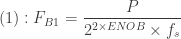
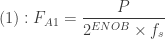
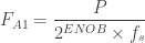
The thermal FOM considers error power rather than amplitude (as in the Walden FOM), and therefore the value of FB1 improves by 4× (rather than 2×) for every additional bit of resolution. This matches the theoretical 4× minimum increase in power if ENOB is limited by kT/C-noise [3] and the architecture remains unchanged [4]. It was shown in [5] that the thermal FOM represents a better description of the state-of-the-art power-resolution tradeoffs according to empirical data than the Walden FOM for ENOB ≥ 9.

As seen in Fig. 1, there is a significant difference between DSM and Nyquist ADCs with respect to FB1. With the exception of two early 14-b designs [6]-[7], the global state-of-the-art is defined entirely by delta-sigma modulator implementations while Nyquist ADCs lag distinctly behind. A possible explanation could be that the thermal FOM favors converters whose power dissipation is truly limited by thermal noise, and that high-resolution ∆-∑ ADCs are more distinctly driven into the thermal noise limit than their Nyquist counterparts. Another point is that many scientific DSM implementations use an off-chip (i.e., zero power) decimation filter implemented in software. This will give DSM an unfair advantage over Nyquist, although it can hardly be the only explanation for a one order of magnitude FOM difference.

Since the thermal FOM for Nyquist converters has evolved over a rather uneven path, I’ll not make any elaborate interpretations of its shape. The trend (dashed) is simply fitted to all the state-of-the-art points from 1982–2012, revealing an average improvement rate of 2× every two years. The DSM envelope appears to have three main segments with breakpoints at 1990 and 2000, respectively. For simplicity, a single trend was estimated for the envelope until Naiknaware [8], after which the thermal FOM has evolved significantly slower. From Fiedler [9] to Naiknaware, the average improvement rate is 2× every 17 months (1.4 years) – again faster than Moore’s Law [10]-[11] – whereas from year 2000 to present day [12], the state-of-the-art points fit to a more modest /5.5 years slope. Even if the latter is from a fit of only four data points, and the exact slopes can be discussed, it is clear from Fig. 2 that the thermal FOM for DSM experienced a distinct slowdown after year 2000. This coincides with the breakpoint where the relative noise floor – approximately the denominator in (1) – also goes into saturation. It can further be noticed that it coincides with the accelerated evolution of FA1 as well. A possible, but perhaps speculative interpretation is that the ADC community first focused on thermal noise performance and related design optimization, and after hitting the noise floor around year 2000 moved on to focus on power efficiency.

If you wish to suggest other explanations, please share them below.

This concludes a series of ten posts on ADC performance and technology trends. If you want to go back and read them all from the beginning, these are the topics and the order in which they were posted:

  1. CMOS node adoption
  2. Low-voltage operation – part 1
  3. Low-voltage operation – part 2
  4. Thermal noise
  5. Jitter
  6. Relative noise floor
  7. Linearity (SFDR)
  8. Sampling rate and resolution
  9. Walden FOM
  10. Thermal FOM (this post)

As a small postlude, a follow-up post will list known prior art ADC surveys for those of you that (like myself) have an insatiable appetite for technology trend estimations and empirical data dots.

See also …

ADC survey data

References

  1. A. M. A. Ali, C. Dillon, R. Sneed, A. S. Morgan, S. Bardsley, J. Kornblum, and L. Wu, “A 14-bit 125 MS/s IF/RF sampling pipelined ADC with 100 dB SFDR and 50 fs jitter,” IEEE J. Solid-State Circuits, Vol. 41, pp. 1846–1855, Aug, 2006.
  2. C. Wulff, and T. Ytterdal, “Design of a 7-bit, 200MS/s, 2mW pipelined ADC with switched open-loop amplifiers in a 65nm CMOS technology,” Proc. of NORCHIP, Aalborg, Denmark, Nov., 2007.
  3. B. Murmann, “A/D converter trends: Power dissipation, scaling and digitally assisted architectures,” Proc. of IEEE Custom Integrated Circ. Conf. (CICC), San Jose, California, USA, pp. 105–112, Sept., 2008.
  4. K. Bult, “Embedded analog-to-digital converters,” Proc. of Eur. Solid-State Circ. Conf. (ESSCIRC), Athens, Greece, pp. 52–60, Sept., 2009.
  5. B. E. Jonsson, “Using Figures-of-Merit to Evaluate Measured A/D-Converter Performance,” Proc. of 2011 IMEKO IWADC & IEEE ADC Forum, Orvieto, Italy, pp. 1–6, June 2011. [PDF @ IMEKO]
  6. R. J. van de Plassche, and H. J. Schouwenaars, “A Monolithic 14 Bit A/D Converter,” IEEE J. Solid-State Circuits, Vol. SC-17, pp. 1112-1117, Dec., 1982.
  7. T. Sugawara, M. Ishibe, H. Yamada, S.-I. Majima, T. Tanji, and S. Komatsu, “A Monolithic 14 Bit/20 µs Dual Channel A/D Converter,” IEEE J. Solid-State Circuits, Vol. SC-18, pp. 723-729, Dec., 1983.
  8. R. Naiknaware, and T. Fiez, “142dB ∆∑ ADC with a 100nV LSB in a 3V CMOS Process,” Proc. of IEEE Custom Integrated Circ. Conf. (CICC), Orlando, USA, pp. 5–8, May, 2000.
  9. H. L. Fiedler, and B. Hoefflinger, “A CMOS Pulse Density Modulator for High-Resolution A/D Converters,” IEEE J. Solid-State Circuits, Vol. SC-19, pp. 995-996, Dec., 1984.
  10. G.E. Moore, “Cramming more components onto integrated circuits,” Electronics, Vol. 38, No. 8, Apr. 1965.
  11. G. E. Moore, “No exponential is forever: but “forever” can be delayed!,” IEEE ISSCC, Dig. Tech. Papers, San Francisco, CA, Feb. 2003, pp. 20–23.
  12. J. Xu, X. Wu, M. Zhao, R. Fan, H. Wang, X. Ma, and B. Liu, “Ultra Low-FOM High-Precision ΔΣ Modulators with Fully-Clocked SO and Zero Static Power Quantizers,” Proc. of IEEE Custom Integrated Circ. Conf. (CICC), San Jose, California, USA, pp. 1–4, Sept., 2011.

ADC performance evolution: Walden figure-of-merit (FOM)


Figure 1. Evolution of best reported Walden FOM for delta-sigma modulators (o) and Nyquist ADCs (#). Monotonic state-of-the-art improvement trajectories have been highlighted. Trend fit to DSM (dotted), and Nyquist (dashed) state-of-the-art. Average trend for all designs (dash-dotted) included for comparison.

POWER EFFICIENCY TRENDS: A series of blog posts on A/D-converter performance trends would not be complete without an analysis of figure-of-merit (FOM) trends, would it? We will therefore take a look at the two most commonly used FOM, starting with the by far most popular:

(1) : F_{A1} = \dfrac{P}{{2}^{ENOB}\times f_{s}}

where P is the power dissipation, fs is Nyquist sampling rate, and ENOB is the effective number of bits defined by the signal-to-noise and-distortion ratio (SNDR) as:

(2) : ENOB = \dfrac{SNDR - 1.76}{6.02}

FA1 is sometimes referred to as the Walden or ISSCC FOM and relates the ADC power dissipation to its performance, represented by sampling rate and conversion error amplitude. The best reported FA1 value each year has been plotted for delta-sigma modulators (DSM) and Nyquist ADCs in Fig. 1. Trajectories for state-of-the-art have been indicated, and trends have been fitted to these state-of-the-art data points. The average improvement trend for all ADCs (2×/2.6 years) is included for comparison.

By dividing the data into DSM and Nyquist subsets, it is seen that delta-sigma modulators have improved their state-of-the-art FOM at an almost constant rate of 2×/2.5 years throughout the existence of the field – just slightly faster than the overall average. State-of-the-art Nyquist ADCs have followed a steeper and more S-shaped evolution path. Their overall trend fits to a 2× improvement every 1.8 years, although it is obvious that evolution rates have changed significantly over time. A more accurate analysis of Nyquist ADC trends should probably make individual fits of the early days glory, the intermediate slowdown, and the recent acceleration phase. This was done in [1] where evolution was analyzed with DSM and Nyquist data merged. However, for simplicity I’ll just stick to the more conservative overall Nyquist trend. [I wouldn’t want anyone to suggest that I’m producing “subjective” or “highly speculative” trend estimates, would I? 😉 ]

Still, if anyone is curious to know … 🙂 … the state-of-the-art data points fit to a 2×/14 months trend between 2000 and 2010. That’s actually faster than Moore’s Law, which is traditionally attributed a 2×/18 months rate [2]-[3]. A new twist on “More than Moore”, perhaps? Even the more conservative overall 2×/21 months trend is close enough to conclude that the state-of-the-art FOM for Nyquist ADCs has developed exponentially in a fashion closely resembling Moore’s Law. And that’s got to be an impressive trend for any analog/mixed circuit performance parameter.

Irrespective of what’s the best fit to data, it should be evident from Fig. 1 that Nyquist ADCs broke away from the overall trend around year 2000, and has since followed a steeper descent in their figures-of-merit. They have also reached further (4.4 fJ) [4] than DSM (35.6 fJ) [5]. The overall trend projects to a 0.2 fJ ADC FOM in 2020. Whether or not that’s possible, we’ll leave for another post. A deeper look at the data also reveals that:

  • The acceleration in state-of-the-art is almost completely defined by successive-approximation (SAR) ADCs [4], [6]-[11], accompanied by a single cyclic ADC [12]. The superior energy efficiency of the SAR architecture was empirically shown in [13].
  • A significant part of the acceleration can be explained by the increased tendency to leave out, for example I/O power dissipation when reporting experimental results – a trend also observed by Bult [14]. The FOM in the graph was intentionally calculated from the on-chip rather than total power dissipation because: (a) ADCs are increasingly used as a system-on-chip (SoC) building block, which makes the stand-alone I/O power for a prototype irrelevant, and (b) Many authors don’t even report the I/O power anymore.
  • FA1 has a bias towards low-power, medium resolution designs rather than high-resolution, and thus benefits from CMOS technology scaling as shown in [15],[16]. An analysis of the underlying data shows that, for the best FA1 every year, the trajectories for ENOB and P follows distinct paths towards consistently lower power and medium resolution. You simply gain more in FA1 by lowering power dissipation than by increasing resolution because (1) does not correctly describe the empirically observed power-resolution tradeoff for ADCs [13],[15].

In order to compare high-resolution ADCs limited by thermal noise, it has therefore been proposed to use a slightly different FOM, sometimes labeled the “Thermal FOM” [17]-[18],

(3) : F_{B1} = \dfrac{P}{{2}^{2\times ENOB}\times f_{s}}

This figure-of-merit will be the topic of the next post.

See also …

ADC survey data

Walden’s survey [19]

References

  1. B. E. Jonsson, “A survey of A/D-converter performance evolution,” Proc. of IEEE Int. Conf. Electronics Circ. Syst. (ICECS), Athens, Greece, pp. 768–771, Dec., 2010.
  2. G.E. Moore, “Cramming more components onto integrated circuits,” Electronics, Vol. 38, No. 8, Apr. 1965.
  3. G. E. Moore, “No exponential is forever: but “forever” can be delayed!,” IEEE ISSCC, Dig. Tech. Papers, San Francisco, CA, Feb. 2003, pp. 20–23.
  4. M. van Elzakker, E. van Tuijl, P. Geraedts, D. Schinkel, E. Klumperink, and B. Nauta, “A 1.9μW 4.4fJ/Conversion-step 10b 1MS/s Charge-Redistribution ADC,” Proc. of IEEE Solid-State Circ. Conf. (ISSCC), San Francisco, California, pp. 244–245, Feb., 2008.
  5. J. Xu, X. Wu, M. Zhao, R. Fan, H. Wang, X. Ma, and B. Liu, “Ultra Low-FOM High-Precision ΔΣ Modulators with Fully-Clocked SO and Zero Static Power Quantizers,” Proc. of IEEE Custom Integrated Circ. Conf. (CICC), San Jose, California, USA, pp. 1–4, Sept., 2011.
  6. A. Shikata, R. Sekimoto, T. Kuroda, and H. Ishikuro, “A 0.5 V 1.1 MS/sec 6.3 fJ/Conversion-Step SAR-ADC With Tri-Level Comparator in 40 nm CMOS,” IEEE J. Solid-State Circuits, Vol. 47, pp. 1022–1030, Apr., 2012.
  7. T.-C. Lu, L.-D. Van, C.-S. Lin, C.-M. Huang, “A 0.5V 1KS/s 2.5nW 8.52-ENOB 6.8fJ/Conversion-Step SAR ADC for Biomedical Applications,” Proc. of IEEE Custom Integrated Circ. Conf. (CICC), San Jose, California, USA, pp. 1–4, Sept., 2011.
  8. S.-K. Lee, S.-J. Park, Y. Suh, H.-J. Park, and J.-Y. Sim, “A 1.3µW 0.6V 8.7-ENOB Successive Approximation ADC in a 0.18µm CMOS,” Symp. VLSI Circ. Digest of Technical Papers, Honolulu, USA, pp. 242–243, June, 2009.
  9. H.-C. Hong, and G.-M. Lee, “A 65-fJ/Conversion-Step 0.9-V 200-kS/s Rail-to-Rail 8-bit Successive Approximation ADC,” IEEE J. Solid-State Circuits, Vol. 42, pp. 2161–2168, Oct., 2007.
  10. M. D. Scott, B. E. Boser, and K. S. J. Pister, “An Ultra-Low Power ADC for Distributed Sensor Networks,” Proc. of Eur. Solid-State Circ. Conf. (ESSCIRC), Firenze, Italy, pp. 255–258, Sept., 2002.
  11. M. D. Scott, B. E. Boser, and K. S. J. Pister, “An Ultralow-Energy ADC for Smart Dust,” IEEE J. Solid-State Circuits, Vol. 38, pp. 1123–1129, July, 2003.
  12. D. Muthers, and R. Tiekert, “A 0.11mm2 low-power A/D-converter cell for 10b 10MS/s operation,” Proc. of Eur. Solid-State Circ. Conf. (ESSCIRC), Leuven, Belgium, pp. 251–254, Sept., 2004.
  13. B. E. Jonsson, “An empirical approach to finding energy efficient ADC architectures,” Proc. of 2011 IMEKO IWADC & IEEE ADC Forum, Orvieto, Italy, pp. 1–6, June 2011. [PDF @ IMEKO]
  14. K. Bult, “Embedded analog-to-digital converters,” Proc. of Eur. Solid-State Circ. Conf. (ESSCIRC), Athens, Greece, pp. 52–60, Sept., 2009.
  15. B. E. Jonsson, “Using Figures-of-Merit to Evaluate Measured A/D-Converter Performance,” Proc. of 2011 IMEKO IWADC & IEEE ADC Forum, Orvieto, Italy, pp. 1–6, June 2011. [PDF @ IMEKO]
  16. B. E. Jonsson, “On CMOS scaling and A/D-converter performance,” Proc. of NORCHIP, Tampere, Finland, Nov. 2010.
  17. A. M. A. Ali, C. Dillon, R. Sneed, A. S. Morgan, S. Bardsley, J. Kornblum, and L. Wu, “A 14-bit 125 MS/s IF/RF sampling pipelined ADC with 100 dB SFDR and 50 fs jitter,” IEEE J. Solid-State Circuits, Vol. 41, pp. 1846–1855, Aug, 2006.
  18. C. Wulff, and T. Ytterdal, “Design of a 7-bit, 200MS/s, 2mW pipelined ADC with switched open-loop amplifiers in a 65nm CMOS technology,” Proc. of NORCHIP, Aalborg, Denmark, Nov., 2007.
  19. R. Walden, “Analog-to-digital conversion in the early twenty-first century,” Wiley Encyclopedia of Computer Science and Engineering, pp. 126–138, Wiley, 2008.

ADC performance evolution: Sampling rate and resolution


ENOB-vs-fs evolution front

Figure 1. Evolution of ENOB vs. fs envelope for scientifically reported ADCs. Current state-of-the art is compared to state-of-the-art envelopes at 1990 (#) and 2000 (<). Theoretical limits for thermal noise @ VFS = 1V (dotted) and jitter (dashed) are indicated.

SPEED/RESOLUTION TRENDS: Previous posts analyzed noise and linearity separately. Another common approach is to review the overall ADC performance in terms of sampling rate and effective resolution ENOB. In Fig. 1, the current state-of-the-art at ~Q1-2012 is compared to the envelopes for 1990 and 2000 in order to show the simultaneous evolution of the two parameters throughout the entire parameter space. SNR-only results have been excluded from this plot because ENOB is not fully defined by SNR. Hence, there is no experimental data available before 1980. By 1990 the curve has assumed the expected shape. Between 1990 and 2000 there is a 1-4 bits improvement across the full range of sampling rates. The main advances were in the 200kS/s – 100MS/s speed range. This corresponds to typical telecommunications specifications – from single-carrier GSM to multi-carrier WCDMA receivers. From year 2000 to present day, the more significant advances were at 12.5 MS/s [1], from 100–250 MS/s, [2]-[3], at 3 GS/s [4], and above 10 GS/s [5]-[7].

The thermal noise limits according to equation (4) in the thermal noise post have been included as a visual guide, using VFS = 1V, = 300 K, and Rn = {50, 2000} Ω. Similarly, the theoretical jitter-limited ENOB at fin fs/2 according to equation (1) in the jitter post has been added for σt = {0.1, 1, 10} ps. The Rn and σt values were deliberately chosen to simplify comparison with a similar plot in Walden’s survey [8] (see also Additional remarks below). Although the jitter limits should preferably be observed from SNR vs. fin (as done in the post on jitter trends), the shape of the state-of-the-art envelopes in Fig. 1 clearly indicate the regions where ADC performance is limited by thermal noise and jitter respectively. The design by Naiknaware et al. [10] is limited by thermal noise, while those by Poulton et al. [5] and Greshishchev et al. [7] are limited by sampling jitter (and/or metastability [9]). At the boundary between thermal noise and jitter limited designs are the ADCs that suffer from both noise sources in equal amount, such as the design by Ali et al. [3]. Designs in this corner put strict demands on the simultaneous design for jitter and thermal noise.

In the next post will take a look at the trends for ADC FOM.

Additional remarks

  • It may seem that the state-of-the-art thermal noise according to Fig. 1 is equivalent to less than 2 kΩ for some designs. This would obviously be in contradiction to the 2.5 and 6.2 kΩ state-of-the-art reported for delta-sigma modulator and Nyquist ADCs, respectively. The thermal noise limits in Fig. 1 are only valid for VFS = 1 Vpp, and the apparently better results here are because of a larger full-scale range, e.g., 2.5 V for [3]. The correct noise-resistance estimations are found here.
  • The corresponding jitter limits in [8] have a 0.5-bit offset because it appears that Walden derives the rms-signal to peak-noise ratio by assuming that the signal is always sampled where the slope is greatest, i.e., in the zero-crossings [9]. In reality, the signal is sampled anywhere along the waveform for all but pathological cases, and therefore the rms slope should be used instead, as was done in this treatment.
  • In [11], the evolution trends for peak sampling rate at fixed minimum ENOB grades {4, 8, 12, 14} bits, and the complementary peak ENOB at fixed minimum sampling rates {10k, 100k, 1M, 100M, 1G} S/s are shown in a style similar to Fig. 3 in the previous post.

See also …

ADC performance evolution: Linearity (SFDR)

ADC performance evolution: Thermal noise

ADC performance evolution: Jitter

ADC performance evolution: Relative noise floor

ADC survey data

References

  1. C. P. Hurrell, C. Lyden, D. Laing, D. Hummerston, and M. Vickery, “An 18 b 12.5 MS/s ADC With 93 dB SNR,” IEEE J. Solid-State Circuits, Vol. 45, pp. 2647–2654, Dec., 2010.
  2. S. Devarajan, L. Singer, D. Kelly, S. Decker, A. Kamath, and P. Wilkins, “A 16b 125MS/s 385mW 78.7dB SNR CMOS pipeline ADC,” Proc. of IEEE Solid-State Circ. Conf. (ISSCC), San Francisco, California, pp. 86–87, Feb., 2009.
  3. A. M. A. Ali, A. Morgan, C. Dillon, G. Patterson, S. Puckett, P. Bhorashkar, H. Dinc, M. Hensley, R. Stop, S. Bardsley, D. Lattimore, J. Bray, C. Speir, and R. Sneed, “A 16-bit 250-MS/s IF Sampling Pipelined ADC With Background Calibration,” IEEE J. Solid-State Circuits, Vol. 45, pp. 2602-2612, Dec., 2010.
  4. C.-Y. Chen, and  J. Wu, “A 12b 3GS/s Pipeline ADC with 500mW and 0.4 mm2 in 40nm Digital CMOS,” Symp. VLSI Circ. Digest of Technical Papers, Kyoto, Japan, pp. 120–121, June, 2011.
  5. K. Poulton, R. Neff, B. Setterberg, B. Wuppermann, T. Kopley, R. Jewett, J. Pernilo, C. Tan, and A. Montijo, “A 20GS/s 8b ADC with a 1MB memory in 0.18μm CMOS,” Proc. of IEEE Solid-State Circ. Conf. (ISSCC), San Francisco, California, pp. 318–319, Feb., 2003.
  6. S. Shahramian, S. P. Voinigescu, and A. C. Carusone, “A 35-GS/s, 4-bit flash ADC with active data and clock distribution trees,” IEEE J. Solid-State Circuits, Vol. 44, pp. 1709–1720, June, 2009.
  7. Y. M. Greshishchev, J. Aguirre, M. Besson, R. Gibbins, C. Falt, P. Flemke, N. Ben-Hamida, D. Pollex, P. Schvan, and S.-C. Wang, “A 40GS/s 6b ADC in 65nm CMOS,” Proc. of IEEE Solid-State Circ. Conf. (ISSCC), San Francisco, California, pp. 390–391, Feb., 2010.
  8. R. Walden, “Analog-to-digital conversion in the early twenty-first century,” Wiley Encyclopedia of Computer Science and Engineering, pp. 126–138, Wiley, 2008.
  9. R. H. Walden, “Analog-to-digital converter survey and analysis,” IEEE J. Selected Areas in Communications, no. 4, pp. 539–550, Apr. 1999.
  10. R. Naiknaware, and T. Fiez, “142dB ∆∑ ADC with a 100nV LSB in a 3V CMOS process,” Proc. of IEEE Custom Integrated Circ. Conf. (CICC), Orlando, USA, pp. 5–8, May, 2000
  11. B. E. Jonsson, “A survey of A/D-converter performance evolution,” Proc. of IEEE Int. Conf. Electronics Circ. Syst. (ICECS), Athens, Greece, pp. 768–771, Dec., 2010.

ADC performance evolution: Relative noise floor


Figure 1. Evolution of relative noise-floor for DSM (o) and Nyquist (#) ADCs over time.

WHAT YOU SEE IS WHAT YOU GET: We have previously studied the evolution of absolute thermal noise levels, and sampling jitter for analog-to-digital converters (ADC). Finally, the overall noise performance evolution is observed with all noise contributors included. Whereas the two previous posts analyzed two fundamental noise components in isolation, this post looks at the actual noise performance achieved with everything included. This is the ADC performance you actually get.

Observation of ADC noise floor trends

The ADC survey data spans a very wide range of converter specifications. An SNR of x dB in 20 kHz bandwidth is not as impressive as achieving the same in a 1GHz band. Using the relative noise-floor nr in dB/Hz derived by (1) allow ADCs with widely different Nyquist bandwidths (BW) to be compared with respect to noise performance.

(1) : n_{r}= - ( SNR+10\times\log_{10}BW )

Figure 1 shows the evolution of nr for delta-sigma modulators (DSM) and Nyquist ADCs over time. A similar plot, based on less data, and not differentiating between DSM and Nyquist ADCs is found in [1]. From a linear fit of the state-of-the-art data points, it is seen here that ADC noise-floor for has evolved at an average rate of ~2.2 dB/year until year 2000 for DSM, after which it has remained in saturation. Nyquist ADCs have developed at a slower rate of ~1.3 dB/year until 2010. The current state-of-the-art is approximately the same for both: –162 dB/Hz for DSM [2], and –161 dB/Hz for Nyquist [3]. Since the state-of-the-art for Nyquist converters was so recently reported, it cannot be concluded only from Fig. 1 that the noise floor for Nyquist ADCs is in saturation. A likely explanation for the DSM trend is, however, the lower signal swing, and thus higher relative noise-floor, implied by the continuous scaling of semiconductor technology [4],[5]. This is also seen in Fig. 2. Although the absolute noise-floor may remain constant in devices [6], the relative noise-floor is raised when signal swing is reduced. New technologies may allow higher bandwidths, but the simultaneous combination of SNR and bandwidth has not improved for a decade due to this inherent dynamic-range limitation of nanometer technology [5]. It is likely to assume that Nyquist converters will suffer from this limit at least as much as delta-sigma modulators do. Noise-performance normalized to signal bandwidth therefore seems to have reached the physical limits of process technology defined by the available signal swing. Expecting a further reduction in signal swing [9], future ADCs could very well fail to maintain the current state-of-the-art in noise performance.

Figure 2. Evolution of relative noise-floor for DSM (o) and Nyquist (#) ADCs vs. node geometry (any technology).

Conclusion: ADC noise performance trends

Over the last three posts, it was seen that the overall state-of-the-art with respect to absolute noise power, sampling jitter, and relative total noise floor has not improved during the last 5–10 years. It is therefore concluded that all significant aspects of ADC noise performance appear to have reached saturation. This is an expected, yet significant result of the study as it clearly confirms the commonly raised concerns regarding analog design and dynamic range in scaled technologies, e.g., in [4]-[8].

My conclusion is that A/D-converters have already hit the noise floor – at least its softer upper coating.

What do you conclude?

In upcoming parts of the ADC performance evolution series of posts we will next take a look at ADC linearity trends.

Additional remarks

  • As commented in part 1, the trends of degradation observed below 65 nm in Fig. 2 may be due to lack of reported attempts, and not necessarily due to physics.
  • Using a circuit design that allows for large input signal swing can help a lot in improving relative noise floor performance. As an example, the state-of-the-art design by Hurrell et al. [3] reports an 8.2 V peak-to-peak input full-scale range.

See also …

ADC performance evolution: Thermal noise

ADC performance evolution: Jitter

ADC performance evolution: Low-voltage operation – part 1

ADC performance evolution: Low-voltage operation – part 2

ADC survey data

References

  1. B. E. Jonsson, “A survey of A/D-converter performance evolution,” Proc. of IEEE Int. Conf. Electronics Circ. Syst. (ICECS), Athens, Greece, pp. 768–771, Dec., 2010.
  2. R. Naiknaware, and T. Fiez, “142dB ∆∑ ADC with a 100nV LSB in a 3V CMOS Process,” Proc. of IEEE Custom Integrated Circ. Conf. (CICC), Orlando, USA, pp. 5-8, May, 2000.
  3. C. P. Hurrell, C. Lyden, D. Laing, D. Hummerston, and M. Vickery, “An 18 b 12.5 MS/s ADC With 93 dB SNR,” IEEE J. Solid-State Circuits, Vol. 45, pp. 2647-2654, Dec., 2010.
  4. K. Bult, “Analog design in deep sub-micron CMOS,” Proc. of Eur. Solid-State Circ. Conf. (ESSCIRC), Stockholm, Sweden, pp. 126–132, Sept., 2000.
  5. B. E. Jonsson, “On CMOS scaling and A/D-converter performance,” Proc. of NORCHIP, Tampere, Finland, Nov. 2010.
  6. W. Sansen, “Analog design challenges in nanometer CMOS technologies,” Proc. of IEEE Asian Solid-State Circ. Conf. (ASSCC), Jeju, Korea, pp. 5–9, Nov., 2007.
  7. B. Murmann, “A/D converter trends: Power dissipation, scaling and digitally assisted architectures,” Proc. of IEEE Custom Integrated Circ. Conf. (CICC), San Jose, California, USA, pp. 105–112, Sept., 2008.
  8. Y. Chiu, B. Nicolic, and P. R. Gray, “Scaling of analog-to-digital converters into ultra-deep-submicron CMOS,” in Proc. Custom Integrated Circuits Conf., San Jose, Sept. 2005, pp. 375–382.
  9. International Technology Roadmap for Semiconductors (ITRS), 2011 Edition [Online]. Available: http://www.itrs.net

The path to a good A/D-converter FOM


Figure 1. ENOB, power, and sampling rate trajectories showing the evolution path to the current state-of-the art FOM.

If you are participating in the scientific competition to report an ever better ADC figure-of-merit (FOM), you will find some pretty useful information in this post. Basically it will tell you where to start “drilling for oil”, and with a bit of persistence (preferably combined with some skill in the art) it might take you all the way to ISSCC 2013. The deadline for ISSCC 2012 is probably a bit too close for anyone to make a full ADC implementation according to these guidelines and still get it back in time from the foundry. But you can always try. I will give you a set of information about design and performance parameters that will enable you to predict quite accurately where in the design space the next state-of-the-art ADC (with respect to FOM) will be located. Remember that it could be your ADC, if you choose to optimize the speed-resolution-power tradeoff for this particular target.

First, let us clarify that we are talking about the most commonly used ADC figure-of-merit of all:

F_{A1} = \dfrac{P}{{2}^{ENOB}\times f_{s}}

Figure 1 illustrates the trajectories of each of the three parameters in FA1 as FA1 improved over time. Click on the image to enlarge it. Only the data points representing an advance of FA1 state-of-the-art, i.e., the monotonic decrease of FA1 over time are used in the plot. Time was also quantized so that only the single best ADC per year appears in the trajectories. The underlying data set is gathered from 1600 scientific papers, and the same as used in [1]-[5]. The FOM axis and the FOM values for each dot are the same for all three plots, while the x axes show the simultaneous values of ENOB, power dissipation and sampling rate, respectively. These are the three parameters used to calculate the FOM, so any systematic trends in their trajectories are likely to be a good direction for a FOM-optimized design.

Figure 2. Approximate trajectory trends suggested by the plots.

Although there is plenty of noise in some of the trajectories, visual inspection suggests the approximate trends indicated in Fig. 2. At least it is my best guesstimate. It is purely ad hoc, and you are of course invited to discuss and refine my estimates by posting comments below. The most obvious trend applies to power dissipation (P), which has reduced by almost six orders of magnitude – from Watts to micro-Watts. At the same time the effective resolution (ENOB) has followed a more noisy, but visible path towards lower (medium) resolutions – from ~14 to currently 9-b ENOB. The change equals a three orders of magnitude increase in error power. Finally, the sampling rates at which state-of-the-art figures-of-merit were achieved have migrated slowly, from ~100 kS/s to 1–10 MS/s, even if state-of-the-art FOMs have occasionally been reported at several GS/s in the past. Looking at the fs trajectory from a purely mathematical curve-fitting perspective, it would not support the trend suggested by the green curve. Weighing in some understanding of the speed-power tradeoff in actual design (described below), it makes a bit more sense. It appears thus, that the FOM is best improved by lowering the power dissipation and accepting a medium resolution, while running at moderate sampling rates.

Understanding the trajectories

In high-resolution ADCs, it can be shown that the power dissipation has a lower limit defined by the size of capacitors sized for a kT/C-noise in line with the target ENOB. The power used to drive these capacitors increase by 4X for every additional bit of resolution – in other words, as {{2}^{2\times ENOB}} 
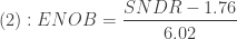
. It was shown in [3] and [4] that the break point where power dissipation becomes proportional to {{2}^{2\times ENOB}} is currently @ 9-b ENOB for the most power efficient ADCs. It was also shown in [4] that FA1 will always have a sweet spot at this break point.

Since FA1 (erroneously) presupposes that P is proportional to {{2}^{ENOB}} (rather than {{2}^{2\times ENOB}} ) for P and ENOB to be traded on equal terms, you will always improve FA1 more by lowering P than by increasing ENOB – as long as ENOB ≥ 9. Below the 9-b break point, state-of-the-art P/fs is approximately independent of ENOB [3]-[4],  which makes it meaningless to lower the resolution further, as it would only diminish the {{2}^{ENOB}} factor in FA1 and do very little to reduce P/fs. This is the reason why the trajectories has not migrated to even lower resolutions and dissipations – for example to a pathologically low ENOB with femto-Watt dissipation.

The reason state-of-the-art FA1 values tend to be reported for 0.1–10 MS/s ADCs is perhaps less obvious. A reasonable assumption is that energy per sample (P/fs) increase faster than linearly with fs when sampling rates are pushed further, and therefore moderately fast designs are likely to have a more optimal P/fs at any fixed ENOB.

Cookbook for an optimized FOM

It was shown in [2] that the state-of-the-art FA1 also improves with every step of CMOS scaling. Including the parameter trajectories showed in this post, the recipe for a good A/D-converter FOM would be something like:

  • Use the most deeply scaled CMOS process you possibly can.
  • Aim for 8–9-b effective resolution, and a modest sampling rate.
  • Use the lowest amount of power that will place you at the ENOB sweet spot, and let the measurements decide exactly what fs you should claim in the paper 😉

There are a few more tricks – some of which can be understood from [3] and some that I’ll save for clients and partners – but that’s more or less it. It will obviously help if you’re prepared to go the extra mile with your design, like the current record holders van Elzakker, et al. [6], who introduced multi-step charging of capacitors to further reduce P/fs. Honing your design skills will help too, but essentially you’re now set to go out and design the next big scientific hit … 

Keep trying, and best wishes! 🙂

References

[1] B. E. Jonsson, “A survey of A/D-converter performance evolution,” Proc. of IEEE Int. Conf. Electronics Circ. Syst. (ICECS), Athens, Greece, pp. 768–771, Dec., 2010.

[2] B. E. Jonsson, “On CMOS scaling and A/D-converter performance,” Proc. of NORCHIP, Tampere, Finland, pp. 1–4, Nov. 2010.

[3] B. E. Jonsson, “An empirical approach to finding energy efficient ADC architectures,” Proc. of 2011 IMEKO IWADC & IEEE ADC Forum, Orvieto, Italy, pp. 1–6, June 2011. [PDF @ IMEKO]

[4] B. E. Jonsson, “Using Figures-of-Merit to Evaluate Measured A/D-Converter Performance,” Proc. of 2011 IMEKO IWADC & IEEE ADC Forum, Orvieto, Italy, pp. 1–6, June 2011. [PDF @ IMEKO]

[5] B. E. Jonsson, “Area Efficiency of ADC Architectures,” Accepted for presentation at Eur. Conf. Circ. Theory and Des. (ECCTD), Linköping, Sweden, Aug., 2011.

[6]    M. van Elzakker, E. van Tuijl, P. Geraedts, D. Schinkel, E. Klumperink, and B. Nauta, “A 1.9μW 4.4fJ/Conversion-step 10b 1MS/s charge-redistribution ADC,” Proc. of IEEE Solid-State Circ. Conf. (ISSCC), San Francisco, California, pp. 244–245, Feb., 2008.